Saltar directamente a la navegación principal Saltar directamente al contenido Saltar a la subnavegación

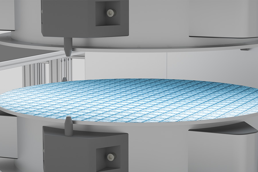
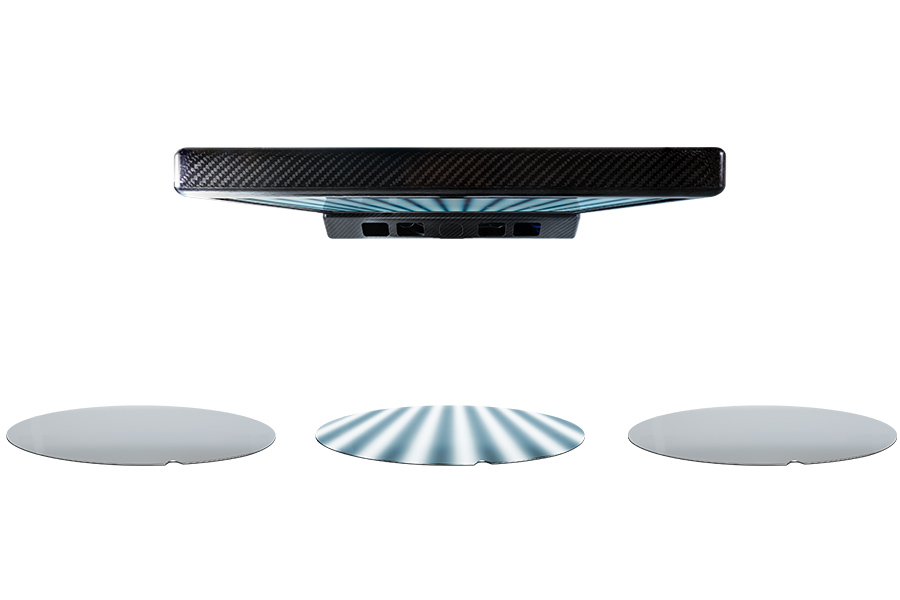
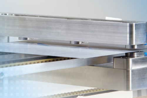
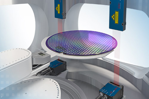
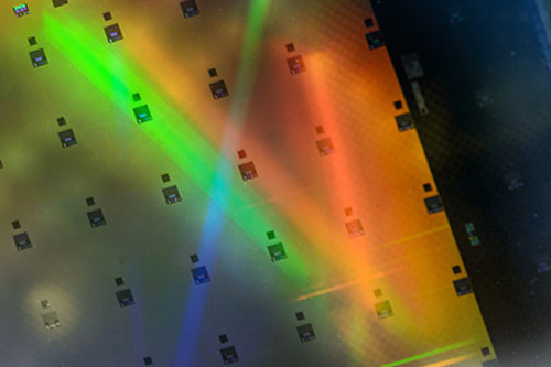
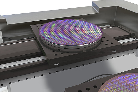
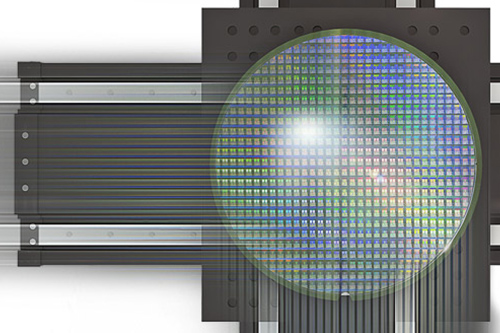
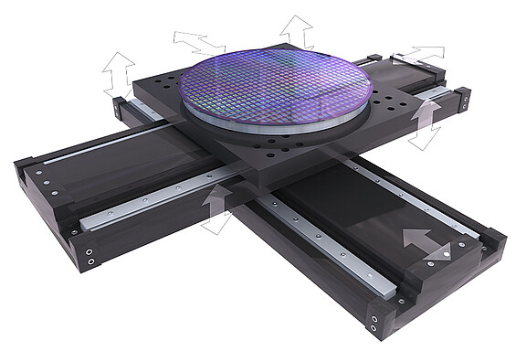
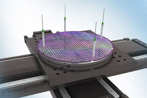
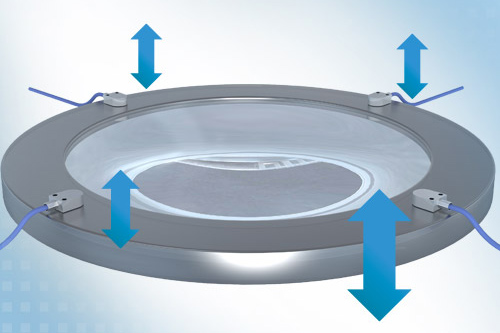
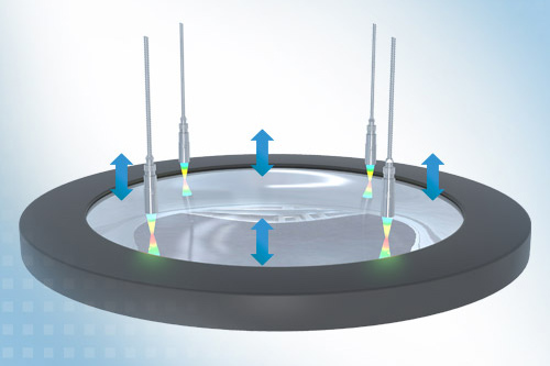
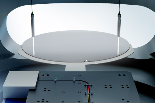
Semiconductores y obleas (wafers)

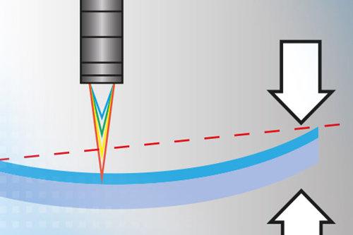
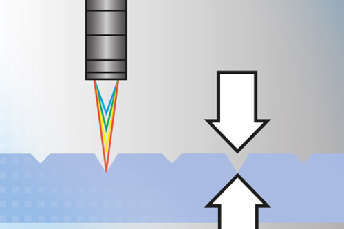
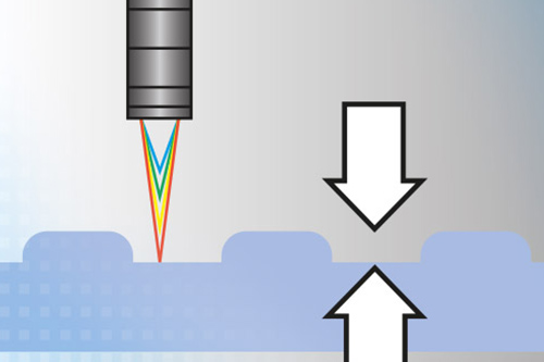
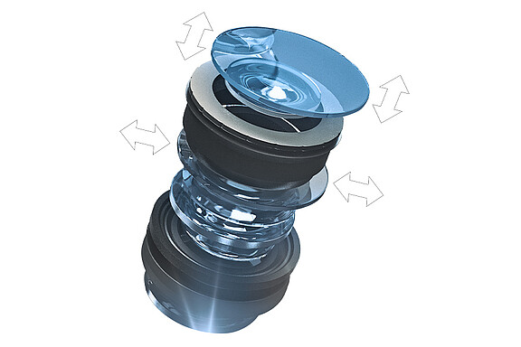
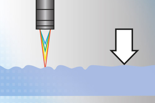
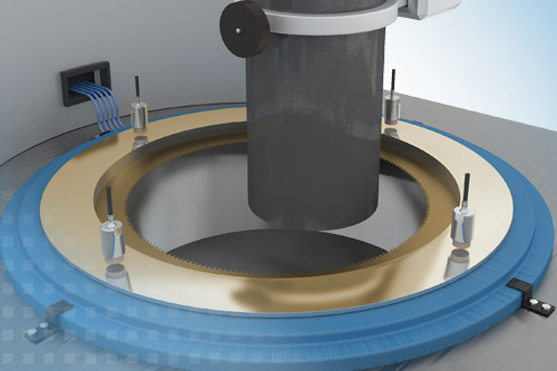
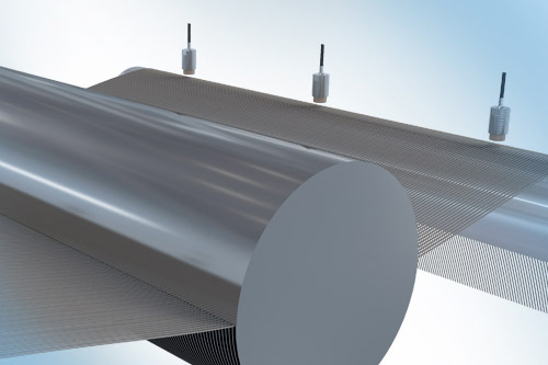
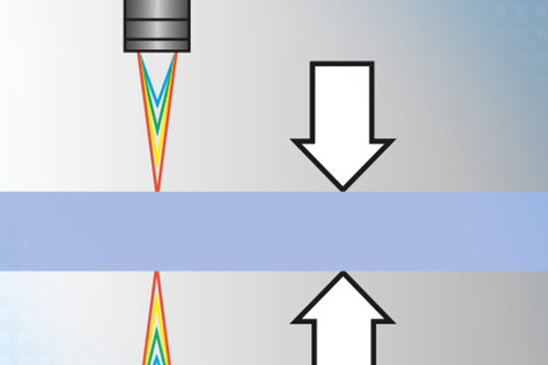
Las operaciones de medición en el sector de los semiconductores requieren máxima precisión y reproducibilidad.

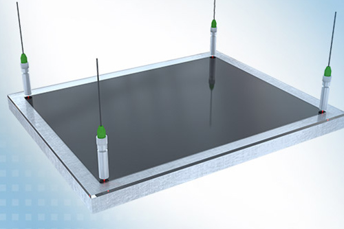
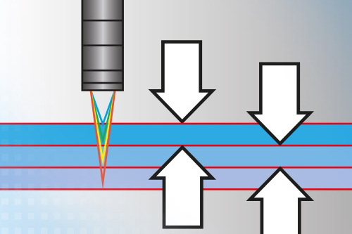
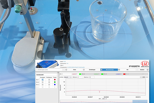
Micro-Epsilon ofrece la solución adecuada para numerosas aplicaciones - desde el posicionamiento preciso de los equipos hasta la inspección de las obleas y la medición topográfica.

3D shape measurement of wafers

reflectCONTROL deflectometry systems are used to detect the flatness or planarity of 150 mm wafers. These measure the flatness with only one image. For this purpose, the sensors project a striped pattern onto the wafer, which is recorded by the…

Más información
Detección de la forma 3D de obleas

High precision thickness measurement of silicon wafers

Capacitive displacement sensors are used for the exact thickness measurement of wafers. Two opposing sensors detect the thickness and also determine other parameters such as deflection or sawing marks. The position of the wafer in the measuring…

Más información
High precision thickness measurement of silicon wafers

Dimensional inspection of silicon ingots

Laser profile scanners from Micro-Epsilon are used to inspect the geometry of silicon ingots. These detect the complete geometry of the silicon rods. This allows geometrical deviations of the silicon block to be determined before separation.…

Más información
Dimensional inspection of silicon ingots

Bow and warp of wafers

Confocal chromatic sensors scan the wafer surface to detect bow, warp and distortion. Providing high measuring rates, confocalDT controllers enable highly dynamic measurements, allowing the wafer to be inspected within short cycle times. …

Más información
Bow and warp

Detection and measurement of saw marks

For automatic detection and measurement of saw marks, confocal chromatic sensors from Micro-Epsilon are used. The fast surface compensation feature of the controller regulates the exposure cycles in order to achieve maximum signal stability on…

Más información
Detection and measurement of saw marks

Recognition and measurement of bumps on silicon wafers

Confocal chromatic displacement sensors from Micro-Epsilon are used to inspect bumps. They generate a small light spot onto the wafer, while reliably detecting the smallest of parts and structures at high resolutions. Therefore, shape and…

Más información
Detection and measurement of bumps on silicon wafers

Determining the position during wafer handling

When handling wafers, exact and repeatable positioning is crucial. During the infeed of wafers, two optoCONTROL laser micrometers inspect the diameter and thus determine the horizontal position. Thanks to the high measuring rate and accuracy,…

Más información
Position determination during wafer handling

Positioning of masks in lithography

Lithography processes require high resolution and long-term measurement of machine movements in order to achieve maximum precision. High resolutions enable nanometer-precise positioning of masks using capacitive sensors from Micro-Epsilon. Their…

Más información
##NO_MATCH##. High resolutions enable nanometer-precise positioning of masks using capacitive sensors from Micro-Epsilon. Their vacuum-suitable design enables the sensors and cables to be used in ultra-high vacuum. To the product capaNCDT 6200 Applications Industries Additive Manufacturing

White light interferometer for mask positioning in lithography

Lithography processes require high resolution and long-term stable measurement of machine movements in order to achieve maximum precision. Thanks to special evaluation algorithms and active temperature compensation, the IMS5400 white light…

Más información
Interferómetro de luz blanca para el posicionamiento de máscaras en litografía

Transparent layers & adhesive beading

Confocal chromatic sensors are used for one-sided layer thickness measurements. The confocal measuring principle enables the evaluation of several signal peaks, allowing the thickness of transparent materials to be determined. With the multi-peak…

Más información
Transparent layers & adhesive beading

Precise notch detection on glass wafers

The manufacture of high-quality semiconductor chips requires precise alignment and positioning techniques during the production of glass wafers. A crucial step here is notch detection, in which the positions of the notches on the wafer are…

Más información
Precise notch detection on glass wafers

Positioning the wafer stage using capacitive sensors

Capacitive displacement sensors are used for fine positioning tasks in the wafer stage. These sensors measure the position of the stage at various points, which is particularly useful for fine alignment. Thanks to their triaxial design, the…

Más información
Positioning the wafer stage using capacitive sensors

Positioning of the lens system in lithography machines

Non-contact, inductive displacement sensors (eddy current) measure the position of lens elements in order to achieve the highest possible imaging accuracy. Depending on the lens system, displacement sensors from Micro-Epsilon are used to detect…

Más información
Positioning of the lens system in lithography machines

Nanometer positioning in lithography machines

To illuminate individual components on the wafer, the lithographic devices move the wafer to the respective position. Capacitive displacement sensors measure the position of the travel path in order to enable nanometer-accurate positioning. …

Más información
Nanometer positioning in lithography machines

Positioning the wafer stage

Non-contact sensors from Micro-Epsilon are used for position monitoring of the wafer stage, where they measure highly dynamic XYZ movements of the stage which accelerates very rapidly. Capacitive and inductive (eddy current) sensors achieve…

Más información
Wafer stage positioning

Positioning the wafer stage using white light interferometers

The white light interferoMETER IMS5600 from Micro-Epsilon is used for position monitoring of the wafer stage. It measures the XYZ movements of the stage with extremely high accelerations. The high-precision optical measuring system achieves a…

Más información
Colocación de portaoblea con interferómetros de luz blanca

Checking the tilt angle of lens carriers

Capacitive displacement sensors measure the tilt angle of lens carriers to nanometer accuracy. Thanks to the high-precision measurement, a repeatable projection is ensured. Several sensors measure onto the metallic carrier. Their extremely high…

Más información
Inspección de la inclinación del portalentes

Monitoring the alignment of lenses using confocal chromatic sensors

Confocal chromatic sensors are used to measure the alignment of the lens. Several sensors measure directly on the lens to detect the tilt angle to nanometer accuracy. Unlike electromagnetic sensors, confocal chromatic sensors measure reliably…

Más información
Monitoring the alignment of lenses using confocal chromatic sensors

Inspection of the orientation notches on silicon ingots

Ingots are often provided with orientation notches, which are necessary for the alignment of the ingots. Blue laser scanners from Micro-Epsilon are used to inspect the profile of the notches for dimensional accuracy. They detect the notch profile…

Más información
Inspection of the orientation notches on silicon ingots

Inspection of cracks and breakages

Confocal chromatic sensors from Micro-Epsilon are used to detect cracks and other defects on the wafer. They reliably detect surfaces with varying reflection characteristics due to a fast surface compensation feature. An extremely small light…

Más información
Checking for cracks and breaks

Monitoring the axial movement of annular saws

Annular saws are used for cutting silicon ingots. In order to achieve reliable separation of the ingot, the saw blade or holder is monitored using eddy current sensors. Four sensors measure the distance to the support of the saw without contact.…

Más información
Monitoreo del movimiento axial de sierras circulares

Monitoring the deflection of wire saws

Wire saws are used to cut ingots in only one step. Since the wire is subject to strong wear, the wire bed is monitored at several points using non-contact eddy current sensors. These not only detect the wire height on the guide roller but also…

Más información
Monitoreo de la deflexión de sierras de hilo

Monitoring optical systems using wavefront sensors

Shack-Hartmann wavefront sensors from Optocraft measure the alignment state and the imaging quality of the entire optical system. The robust measuring principle allows machine integration and automated measuring sequences, as well as laser beam…

Más información
Monitoring optical systems with wavefront sensors

Tilt angle measurement of wafers

The exact position of the wafer plays an important role in wafer handling. During the infeed of wafers, white light interferometers measure the horizontal tilt angle of wafers. Two interferometers measure onto the wafer. White light…

Más información
Wafer tilt measurement

Wafer thickness measurement / TTV

Confocal chromatic sensors measure the thickness deviation (Total Thickness Variation) and the wafer thickness from both sides. Based on the wafer thickness profile, bow and warp of the wafer can be detected. High measuring rates enable thickness…

Más información
Wafer thickness measurement / TTV