Interferómetro de luz blanca para medición en línea de espesor de obleas de alta precisión
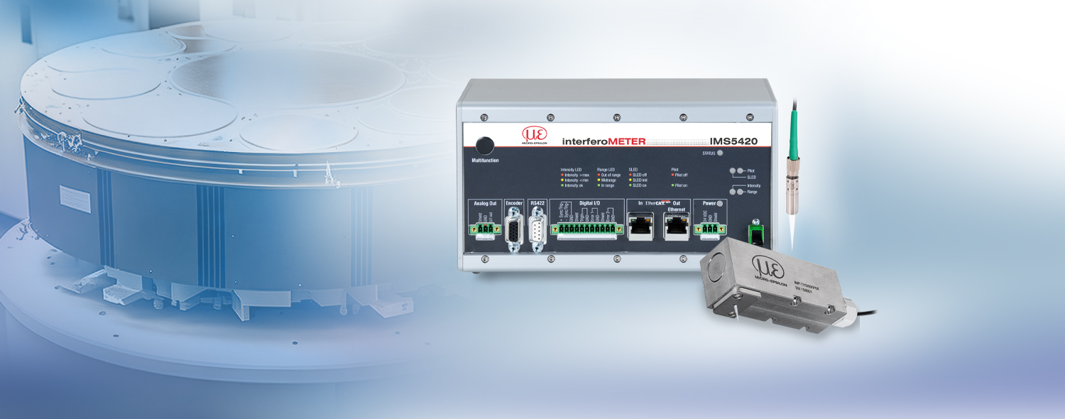
El IMS5420 es un interferómetro de luz blanca de alto rendimiento para medición de espesor sin contacto de obleas de silicio monocristalino. El controlador cuenta con un diodo de superluminiscencia de banda ancha (SLED) con un rango de longitud de onda de 1.100 nm. Este permite la medición de espesor de obleas de silicio no dopadas, dopadas y altamente dopadas con un solo sistema de medición y una estabilidad de señal de menos de 1 nm. Según el ámbito de utilización están disponibles sensores con gran distancia base y sensores con dispositivo de soplado de limpieza.
Characteristics
- Nanometer-accurate thickness measurement of undoped, doped and highly doped wafers
- Multi-peak: acquisition of up to 5 layers with an SI thickness of 0.05 up to 1.05 mm
- High resolution in z-axis of 1 nm
- Measuring rate up to 6 kHz for fast measurements
- Ethernet / EtherCAT / RS422 / PROFINET / EtherNet/IP
- Easy parameterization via web interface
Precise wafer thickness measurement
Due to the optical transparency of silicon wafers in the wavelength range of 1,100 nm, the IMS5420 interferometers can precisely detect the thickness. In this wavelength range, both undoped silicon and doped wafers provide sufficient transparency. Therefore, wafer thicknesses up to 1.05 mm can be detected. The measurable thickness of the air gap is even up to 4 mm.
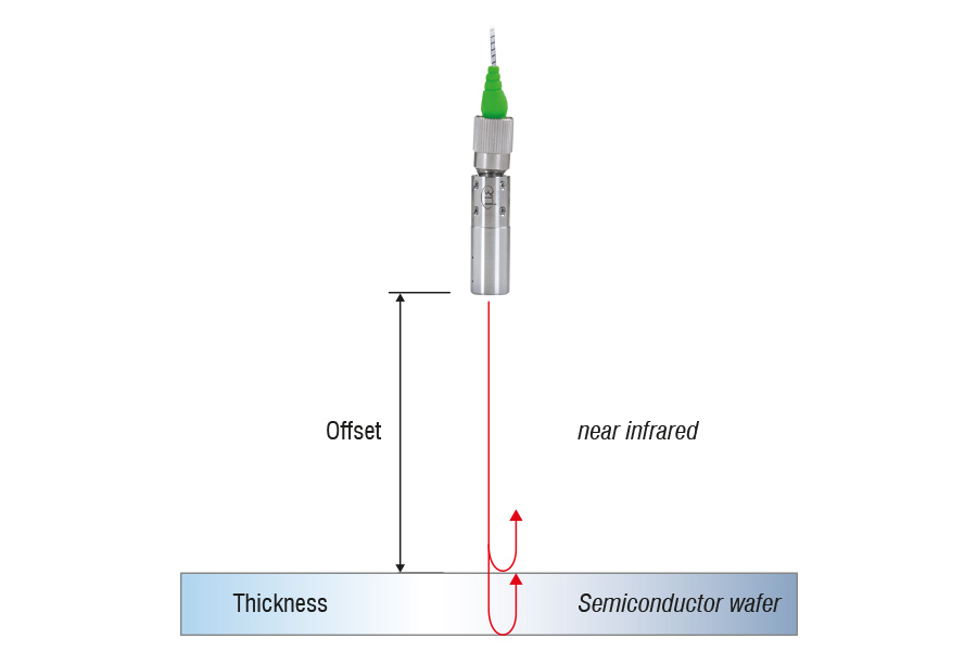
El interferómetro IMS5420 permite medir el espesor de obleas de silicio no dopadas, dopadas y altamente dopadas, y con ello ofrece una gran variedad de aplicaciones. El sistema de medición de espesor de obleas está predestinado para la medición de obleas de silicio monocristalino de un espesor geométrico de 500 a 1050 µm y una dopación de hasta 6 mΩ cm. A pesar de la reducción de la transparencia con el aumento en la dopación, todavía pueden medirse incluso para obleas altamente dopadas espesores de hasta 0,8 mm.
Medición de espesor exacta durante el lapeado
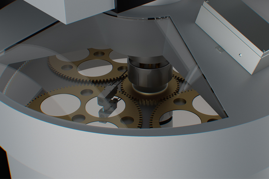
En la fabricación de obleas, primero se corta un lingote de silicio cristalino en discos de aprox. 1 mm de espesor. En el proceso siguiente de rectificado y lapeado, se les da el espesor definido a las obleas, con lo cual se logra al mismo tiempo una alta calidad superficial. Para realizar los procesos de forma estable y reproducible, se integran interferómetros directamente en las máquinas de lapeado y rectificado para medir el espesor en línea. Los valores de espesor registrados se usan tanto para la regulación de la máquina, como también para el aseguramiento de la calidad de cada una de las obleas.
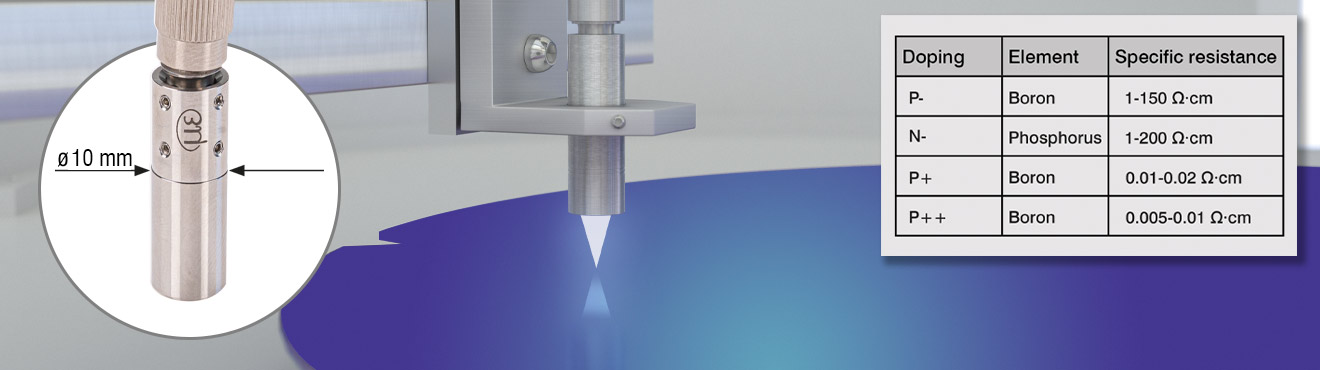
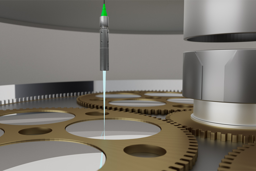
Sensor compacto IMP-NIR-TH24
Con su delgado diámetro de solo 10 mm, y al mismo tiempo con su gran distancia de trabajo de 24 mm, el IMP-NIR-TH24 es ideal para el reequipamiento de las instalaciones existentes. En combinación con el adaptador de montaje ajustable (JMA), se simplifica notablemente la integración, dado que también se pueden compensar de manera confiable las pequeñas desviaciones de montaje o las posiciones oblicuas. A solicitud, están disponibles tanto el sensor como también la fibra óptica del modelo UHV.
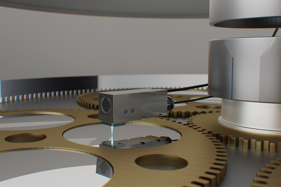
NUEVO: Robusto sensor IMP-NIR-TH3/90/IP68
Con el IMP-NIR-TH3/90/IP68 se amplía la gama de sensores con un potente sensor para situaciones de montaje especialmente exigentes y condiciones ambientales adversas. El sensor convence por su trayectoria del haz de 90° y una pequeña distancia de trabajo de solo 3 mm: ideal para las situaciones de montaje muy estrechas. Además, gracias a su robusta carcasa (IP68), el sensor también es adecuado para utilizarse en aplicaciones especialmente exigentes, como por ejemplo en el rectificado con suspensión abrasiva. El dispositivo de soplado integrado mantiene la trayectoria del haz continuamente libre de suciedad, y permite de esta manera una duradera exactitud de medición, incluso en entornos fuertemente contaminados.
Numerosos modelos para sus exigentes tareas de medición
| Modelo | Distancia de trabajo / rango de medición | Linealidad | Número de capas medibles | Ámbitos de utilización |
|---|---|---|---|---|
| IMS5420-TH | Distancia de trabajo IMP-NIR-TH24 ca. 24 mm (21 … 27 mm) | IMP-NIR-TH3/90/IP68 ca. 3 mm (1 … 6 mm) / 0.05 … 1.05 mm (en silicio / n=3.82), 0.2 … 4 mm (en el aire, n=1) |
< ±100 nm | 1 capa | Medición de espesor en línea, p. ej. tras el rectificado o pulido. |
| IMS5420MP | < ±100 nm con una capa < ±200 nm para otras capas |
hasta 5 capas | Medición de espesor en línea, p. ej. en la revisión de calidad del espesor de capas tras el revestimiento. | |
| IMS5420/IP67 | Distancia de trabajo IMP-NIR-TH24 aprox. 24 mm (21 … 27 mm) / 0.05 … 1.05 mm (en silicio / n=3.82), 0.2 … 4 mm (en el aire, n=1) |
< ±100 nm | 1 capa | Medición industrial de espesor en línea durante el lapeado y rectificado. |
| IMS5420/IP67MP-TH | < ±100 nm en una capa < ±200 nm para otras capas |
hasta 5 capas | Medición industrial de espesor en línea durante el lapeado y rectificado. |
Modern interfaces for integration into machines and systems
The controller offers integrated interfaces such as Ethernet, EtherCAT and RS422 as well as additional encoder connections, analog outputs, synchronization inputs and digital I/Os. When you use Micro-Epsilon's interface modules, PROFINET and EthernetIP are available. This allows the interferometer to be integrated into all control systems and production programs.